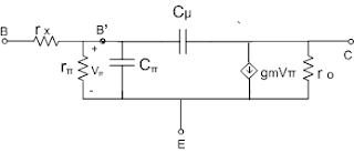
We discussed small signal analysis of BJT under the key word "Small signal analysis". When input signal to an amplifier is in the range of ten to hundred Kilo Hertz, a small signal-low frequency model of the transistor can be used for analysis. But as the frequency increases, internal capacitance of the transistor will strongly effect it's performance. A low frequency model cannot work well in this situation. To accommodate these performance changes of the transistor, a separate model is developed for high frequency operations. This high frequency model is given in Fig 1. A high frequency hybrid-pi model is also known as Giacoletto model.
Low frequency model is given in Fig 2 for quick reference. It is given in the post 'Transistor - small signal model and small signal parameters'. Input resistance (rπ ), Transconductance(gm) and Output resistance (ro) are well explained there. Plz go through it, just to refresh your brain cells.
3) Collector - Base capacitance Cμ
It is the capacitance of the Collector- Base junction of the transistor. It is ranging from fraction of pF to a few pF.
 |
| Fig 1 High frequency model |
 |
| Fig 2 Low frequency model |
Low frequency model is given in Fig 2 for quick reference. It is given in the post 'Transistor - small signal model and small signal parameters'. Input resistance (rπ ), Transconductance(gm) and Output resistance (ro) are well explained there. Plz go through it, just to refresh your brain cells.
High frequency model- explanation
In high frequency model a resistor and two capacitors are added in addition to the components in low frequency model.
1) Resistor rx is known as Base-spreading resistor
In Fig1, B' is a point internal to the transistor and is a part of base region. rx denotes the resistance of the silicon material between external base terminal B and internal base terminal B'. It's value is usually less than 100 ohms and has significant effect in high frequency response. It does not have any roll in low frequency analysis. rx << rπ .
2) Base - Emitter capacitance Cπ
This capacitance occurs due to the combined effect of emitter junction diffusion capacitance Cde and emitter junction depletion capacitance Cje. (Diffusion and depletion capacitance are in your 'Solid State Devices' text book.) It's value is in between few pF to few tens of pF.
It is the capacitance of the Collector- Base junction of the transistor. It is ranging from fraction of pF to a few pF.
 |
| Fig 3 Internal capacitance of BJT |
####Note: In Fig 3, E-B junction is forward biased. Both diffusion and depletion(space charge) capacitance are associated with a forward biased junction. So Cde and Cje forms Cπ. C-B junction is reverse biased and depletion capacitance appear at this junction and is represented as Cμ. ####
For Input resistance (rπ ), Transconductance(gm) and Output resistance (ro) plz use this link.
For Input resistance (rπ ), Transconductance(gm) and Output resistance (ro) plz use this link.